Key Takeaway: Designing your first PCB is a learnable six-step process — and learning how to design a PCB from scratch is easier than ever with free tools like KiCad and EasyEDA that take you from idea to a real board for as little as a few dollars.

Table of Contents
1. Overview
“How do I design a PCB?” is the question every electronics hobbyist asks after their first breadboard project stops being enough. A printed circuit board turns your hand-wired, jumper-filled prototype into a reliable, repeatable artifact — and the practical steps for how to design a PCB are the same whether your budget is zero or corporate. In 2026 you can order five small two-layer boards for under $10 including shipping, so the cost of experimenting is trivial.
This guide is a complete, practical walkthrough of the PCB design process for a complete beginner: choosing free software, drawing a schematic, placing parts, routing traces, running a design rule check, exporting Gerber files, and placing an order. By the end you will understand exactly what happens between the first click in KiCad and the physical board in your mailbox.
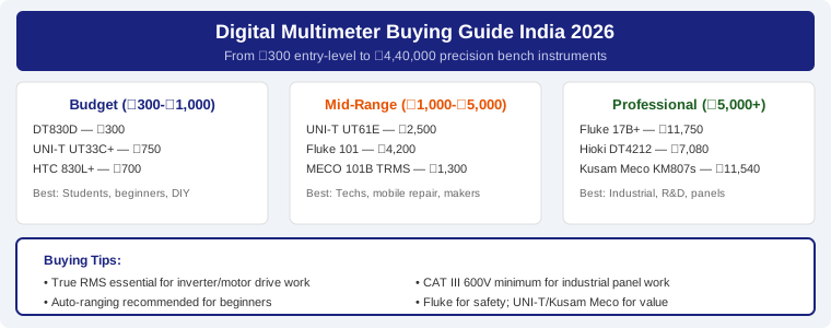
Before you start, make sure the basics on the bench are covered. A good soldering iron and a multimeter will be needed to verify your first board. See our complete digital multimeter guide and our through-hole soldering guide if you have not built that part of your toolbox yet.
2. Choosing Your Software
You do not need expensive software to design a good first PCB. The three tools below cover the whole spectrum from free to professional.
- KiCad — fully open source, runs on Windows, macOS, and Linux, and includes schematic editor, PCB editor, 3D viewer, and Gerber export. The community around KiCad (official site) is huge and beginner tutorials are everywhere.
- EasyEDA — browser-based and extremely beginner friendly, with built-in component libraries and one-click ordering via its own fab service. Start on EasyEDA if you want minimal install friction.
- Fusion 360 / Altium / Allegro — professional tools with steep learning curves and high prices. Skip them for your first board; move up only when you need advanced features like controlled impedance or complex multi-layer stackups.
For this guide, the workflow applies to all of them: schematic to layout to routing to DRC to Gerber to fab.
3. Step 1: Draw the Schematic
The schematic is the logical map of your circuit: components as symbols, connected by wires that carry signals and power. You never draw physical shapes in the schematic editor — only the electrical intent.
- Place symbols for every part: resistors, capacitors, LEDs, the microcontroller or IC, connectors, power input, and decoupling capacitors.
- Wire them together with nets. Give important nets clear names (VCC, GND, SDA, SCL, OUT) so the layout stage is readable.
- Do not skip decoupling capacitors near every IC power pin — 100 nF close to each chip’s VCC is the rule of thumb that saves most first boards from noise problems.
- Run the electrical rules check (ERC). It flags missing connections, unconnected pins, and shorted nets before you ever touch the layout.
If your circuit is an Arduino-, STM32-, or sensor-based project, our I2C communication guide for STM32 and Arduino shows the kind of wiring patterns you will reproduce on a real board.
4. Step 2: Layout and Routing
Now the schematic symbols become physical footprints on a board outline. This is where the design goes from “logical” to “geometric.”
Placement
- Start by placing connectors and mounting holes; they anchor the board mechanically.
- Place the microcontroller in the center, then group supporting parts around it: crystals and their load capacitors near the MCU clock pins, decoupling caps within a few millimeters of each power pin.
- Remember real-world constraints: connectors face the board edge so cables can exit, switches align with enclosure cutouts, and hot or tall parts (transistors on heatsinks, big electrolytics) get clearance.
Routing
- Route short and thick traces for power and ground first. A ground pour (copper fill) on the bottom layer is the single best habit for a first design — it lowers noise and simplifies routing.
- Route signal traces on the top layer, ground fill on the bottom, and use vias to move nets between layers when needed.
- Keep high-speed signals (crystal lines, fast data lines) short and away from noisy inputs. For simple hobby boards this is usually enough.
- Add silkscreen labels for connectors, test points, and polarity marks (LED +/-, capacitor polarity). Future-you will be grateful.
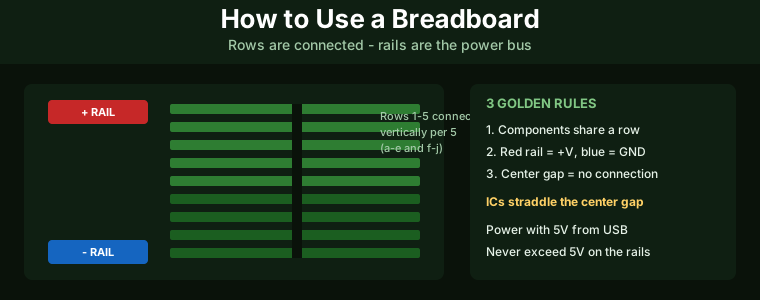
Prototyping on a breadboard first is still the fastest way to validate the circuit. Our breadboard guide for beginners explains how to prove the design works electrically before you commit it to copper.
5. Step 3: Design Rules and DRC
Design rules tell the fab which geometries your board uses, and the design rule check (DRC) verifies the layout against them. Standard budget-fab default rules for a beginner two-layer board:
| Parameter | Typical minimum | Notes |
|---|---|---|
| Trace width | 0.2 mm (8 mil) | Wider for power: 0.5 mm+ for 1 A |
| Clearance | 0.2 mm (8 mil) | Between adjacent traces |
| Drill size | 0.3 mm | Standard vias work at 0.6 mm |
| Board layers | 2 | Top signal + bottom ground/fill |
| Min board size | 10 x 10 cm | Under this = cheapest fab tier |
Run the DRC before exporting. Any error it reports will also be reported by the fab’s own check, and fixing errors at the DRC stage costs minutes instead of a two-week re-order. Getting to your first board with no DRC errors is a genuinely achievable goal for a complete beginner.
6. Steps 4-6: Export Gerbers and Order
With the layout finished and DRC clean, generate the files the factory needs.
- Fanout / review — eyeball the 3D preview (built into KiCad and EasyEDA) to catch parts that overlap or components flipped the wrong way.
- Export Gerber files — one file per layer: top copper, bottom copper, top silk, bottom silk, solder mask top/bottom, and the drill file. Choose the fab’s required format in the export dialog (Gerber X2 or RS-274X is standard).
- Order — upload the Gerber ZIP to your fab. Popular budget options are JLCPCB and PCBWay; they show an instant quote, let you pick color and finish, and panel the board automatically. JLCPCB’s ordering page is a good reference for what the upload flow looks like.
Most fabs also check your files for free and email you a rendering to review before production starts. Always approve visually: traces crossing where they should not, or a missing hole, shows up immediately in their preview.
7. Cost and Lead Times
Pricing for small beginner boards in 2026 is remarkably low. The winning formula is a 10 x 10 cm (or smaller) two-layer board with standard surface finish, ordered with 5-10 copies.
- Boards: around $2-$10 for 5-10 pieces of a small 2-layer board.
- Shipping: $3-$10 depending on destination and speed; slower economy shipping is cheap.
- Lead time: fabrication usually takes 2-5 days plus shipping, so the whole cycle from order to door is about 10-15 days.
- Extra costs to expect: Solder paste stencils ($5-$10, optional for hand soldering), assembly service (only if you outsource), and import duty on larger orders in some countries.
When the boards arrive, solder the components, check voltages before connecting anything delicate, and verify with a multimeter. Our digital multimeter buying guide helps you pick the meter you will use for that verification.
Frequently Asked Questions
How long does it take to learn PCB design?
A complete beginner can go from first opening KiCad to ordering a working two-layer board in about 10-20 hours of focused practice, spread over a weekend or two. Most people succeed on their first or second ordered board, and the design rule check is what makes that possible.
Is it cheaper to design my own PCB or buy a dev board?
For complex microcontrollers with Wi-Fi or Bluetooth, buy a dev board — they cost less than the parts and assembly labor. Design your own PCB when you want a compact, integrated product, specific I/O, or a custom form factor for production.
What software do professionals use for PCB design?
Professionals commonly use Altium Designer, Cadence Allegro, Mentor Xpedition, and Zuken. In the maker and start-up world, KiCad has become increasingly accepted professionally, and EasyEDA and Fusion 360 cover the budget end.
What skills do I need before designing a PCB?
You should be comfortable with basic electronics — Ohm’s law, voltage dividers, how a microcontroller turns an LED on — and have built at least one working circuit on a breadboard. After that, the PCB software teaches you the physical design rules as you go.
Related Reading
- How to Use a Breadboard: Complete Beginner’s Guide
- How to Solder Through-Hole Components: A Beginner’s Guide
- Build a Low-Cost OpenPnP SMT Assembly Line
Sources
- KiCad — Open Source EDA Software
- EasyEDA — Online PCB Design Tool
- JLCPCB — PCB Fabrication and Assembly
Disclosure: This post contains affiliate links. As an Amazon Associate I earn from qualifying purchases. Some fab and software links support the site’s running costs.