Key Takeaway: The STM32V8 is the world’s first microcontroller built on 18nm FD-SOI technology, featuring an Arm Cortex-M85 core running at 800 MHz with 4 MB of embedded phase-change memory (PCM). It exceeds 5,000 points in CoreMark — a 60% boost over the STM32H7 series — and delivers up to 6x faster AI inference for computer vision workloads. Already deployed in SpaceX Starlink satellite laser communication systems, the STM32V8 marks a new era for general-purpose microcontrollers targeting industrial IoT, edge AI, and high-reliability applications.
Table of Contents
1. A New Flagship: The STM32V8 Breakthrough
The STM32V8 microcontroller, announced by STMicroelectronics in late 2025 and entering volume production in Q1 2026, represents the most significant architectural leap in the STM32 family’s two-decade history. Built on an unprecedented 18nm FD-SOI (Fully Depleted Silicon-On-Insulator) process developed in collaboration with Samsung Foundry, the STM32V8 is the first general-purpose microcontroller to combine a Cortex-M85 core running at 800 MHz with 4 MB of embedded phase-change memory (PCM).
The STM32V8 microcontroller delivers a CoreMark score exceeding 5,000 points — a nearly 60% improvement over the STM32H7R/S launched in 2024. This performance gain is not merely incremental; it represents a fundamental shift in what an MCU can achieve. The 18nm process node enables higher transistor density, lower power consumption, and the integration of advanced memory technology that was previously reserved for automotive-grade microcontrollers.
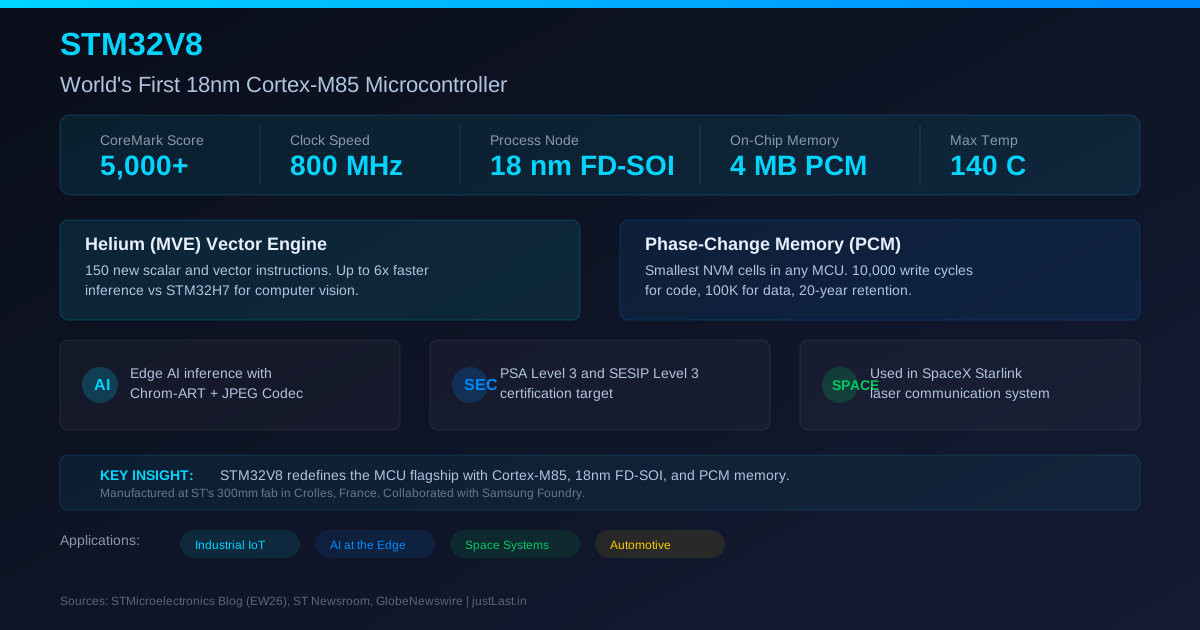
Manufactured at ST’s 300mm fab in Crolles, France, the STM32V8 is produced using a planar process technology that offers significant advantages over FinFET alternatives for mixed-signal MCU designs. Unlike consumer-grade CPUs that use purely digital logic, microcontrollers must integrate analog circuits — ADCs, DACs, comparators, PLLs — which are far more challenging to shrink. ST’s FD-SOI technology uses a thin insulator layer between the source and drain to reduce static leakage, enabling both high performance and low power in a single device rated for up to 140 degrees Celsius junction temperature.
2. Architecture: Cortex-M85 at 800 MHz
The Arm Cortex-M85 core at the heart of the STM32V8 microcontroller represents the most powerful Cortex-M processor available. Based on the Armv8.1-M architecture with a seven-stage pipeline, it offers the best scalar and signal-processing performance of any Cortex-M design. The core includes a Memory Protection Unit (MPU) and an instruction set that optimizes loops and branches through the Armv8-M architecture.
The 800 MHz clock speed is exceptional for a microcontroller, approaching entry-level microprocessor territory. This clock rate enables the STM32V8 to handle compute-intensive tasks like real-time FFT analysis, simultaneous sensor fusion from multiple IMUs, and complex control algorithms without requiring external DSP chips or FPGAs.
The STM32V8 also includes an impressive memory subsystem. The 4 MB of embedded PCM is complemented by significant SRAM for data buffering, and the device supports external memory interfaces for applications requiring additional storage. The dual-bank PCM architecture enables firmware updates without system downtime — critical for mission-critical applications in industrial and aerospace environments.
3. Helium Vector Engine: 6x Faster AI Inference
The M-Profile Vector Extension (MVE), also called Helium technology, is the standout feature for AI and signal processing workloads. Helium adds 150 new scalar and vector instructions that significantly boost performance in machine learning inference and digital signal processing. For developers deploying neural networks at the edge, this means the STM32V8 microcontroller can run inference 6x faster than an STM32H7 running at the same clock speed.
Helium supports half-precision and double-precision floating-point operations with vector integer processing. The 9-to-10 stage vector and floating-point pipeline processes more data per clock cycle, accelerating common ML operations like convolution, pooling, and activation functions. For computer vision applications, this enables real-time object detection and classification directly on the MCU without cloud connectivity.
The ST’s Chrom-ART graphical IP and JPEG Codec further enhance the STM32V8’s multimedia capabilities. Developers can drive displays up to 1280×800 resolution with external RAM, making the chip suitable for advanced graphical user interfaces in industrial HMI panels, medical devices, and smart home control systems.
4. Phase-Change Memory Technology
The most distinctive hardware feature of the STM32V8 microcontroller is its embedded phase-change memory (PCM). Unlike traditional NOR Flash, PCM uses a chalcogenide compound that changes between amorphous and crystalline states in response to temperature changes induced by electrical current pulses. An amorphous state is highly resistive (representing a binary 0), while its polycrystalline phase is highly conductive (representing a binary 1).
ST gained extensive PCM expertise through its Stellar family of automotive microcontrollers, where reliability under extreme conditions is paramount. The move to 18nm made traditional Flash impractical due to cell size limitations, making PCM the ideal choice. Key advantages include:
Density: PCM cells are the smallest non-volatile memory cells in any MCU, halving the footprint compared to MRAM and RRAM alternatives. This allows 4 MB of on-chip storage in a cost-effective die size.
Endurance: PCM supports 10,000 write cycles for code storage and 100,000 cycles for data, with 20 years of data retention. Unlike Flash, PCM does not require erase operations before writes, improving both speed and efficiency.
Radiation Tolerance: PCM is inherently resistant to magnetic fields and radiation, making it ideal for aerospace and defense applications. This was a key factor in SpaceX’s decision to use the STM32V8 in the Starlink satellite constellation.
5. SpaceX Starlink Deployment
The STM32V8 microcontroller has already secured its most prestigious design win: SpaceX selected it for the Starlink mini laser communication system. Low Earth Orbit (LEO) environments are particularly challenging for electronics due to high-radiation conditions, extreme temperature swings, and the need for real-time processing with zero tolerance for failure.
The STM32V8’s combined radiation tolerance, 800 MHz real-time processing capability, and large embedded PCM memory resistant to magnetic fields made it the ideal choice. The Starlink laser links operate at speeds of up to 25 Gbps at distances of 4,000 kilometers, requiring precise timing and control that only a high-performance microcontroller can provide.
SpaceX has also indicated that its teams are evaluating the STM32V8 for additional applications beyond the laser communication system, suggesting that the chip’s reliability in space has exceeded expectations.
6. Target Applications and Ecosystem
While the SpaceX deployment is the headline application, the STM32V8 microcontroller is positioned as a general-purpose flagship targeting a wide range of industries:
Industrial IoT: High-speed data acquisition from multiple sensors, real-time analytics at the edge, and deterministic control of factory automation systems. The 140 degrees Celsius junction temperature rating makes it suitable for harsh manufacturing environments.
Edge AI: On-device machine learning inference for predictive maintenance, quality inspection via computer vision, and anomaly detection in sensor streams. The Helium vector engine enables models that previously required GPU acceleration.
Aerospace and Defense: Radiation-tolerant PCM, high-temperature operation, and real-time determinism make it ideal for satellites, drones, and defense systems where failure is not an option.
Automotive: The STM32V8 targets PSA Level 3 and SESIP Level 3 security certifications, enabling its use in connected vehicle systems, telematics, and advanced driver assistance applications.
Medical Devices: High-precision control for surgical equipment, patient monitoring systems, and diagnostic devices requiring both processing power and reliability.
ST provides a comprehensive ecosystem including the STM32CubeMX2 configuration tool, STM32CubeIDE development environment, HAL2 drivers, and a Discovery Kit with TouchGFX support for GUI development. The STM32V8 is fully supported by FreeRTOS, LwIP, and USBX middleware.
7. STM32V8 vs STM32H7 vs STM32N6
| Feature | STM32V8 | STM32H7R/S | STM32N6 |
|---|---|---|---|
| Core | Cortex-M85 @ 800 MHz | Cortex-M7 @ 600 MHz | Cortex-M55 + NPU |
| Process | 18nm FD-SOI | 40nm | 40nm |
| CoreMark | 5,000+ | ~3,200 | ~2,500 + 600 GOPS NPU |
| On-Chip Memory | 4 MB PCM | Up to 2 MB Flash | Up to 4 MB Flash |
| AI Acceleration | MVE (Helium) | DSP + FPU | Neural-ART NPU |
| Max Temp | 140 C | 125 C | 125 C |
| Security | PSA L3 / SESIP L3 | PSA L1 | PSA L3 / SESIP L3 |
The STM32V8 excels in raw scalar performance and memory density. For applications requiring dedicated neural network acceleration, the STM32N6 with its Neural-ART coprocessor remains the better choice. For most industrial and edge AI applications, the STM32V8’s Helium vector processing provides an excellent balance of performance and programmability.
8. Frequently Asked Questions
What makes the STM32V8 microcontroller different from previous STM32 generations?
The STM32V8 is the first STM32 built on 18nm FD-SOI technology with an 800 MHz Cortex-M85 core and 4 MB of embedded phase-change memory. It exceeds 5,000 CoreMark points — a 60% improvement over the STM32H7 — and delivers up to 6x faster AI inference through the Helium vector engine.
When is the STM32V8 available for purchase?
The STM32V8 entered volume production in Q1 2026. STM32 Nucleo evaluation boards and Discovery Kits are available. Distribution through major electronics distributors like Mouser, DigiKey, and Farnell is underway. Check STMicroelectronics’ website for specific part numbers and pricing.
Can the STM32V8 replace an entry-level microprocessor?
For many applications, yes. The 800 MHz Cortex-M85 with 4 MB PCM memory approaches entry-level MPU territory while maintaining the deterministic real-time behavior and low power consumption of an MCU. Applications that previously required a Linux-capable MPU may now run on the STM32V8 with an RTOS, reducing system complexity and cost.
How does phase-change memory compare to Flash?
PCM offers higher density, faster write speeds (no erase required), better radiation tolerance, and longer endurance in high-temperature environments. The trade-off is slightly higher cost per megabyte compared to mature Flash technology. For mission-critical applications, the advantages far outweigh the cost premium.
What development tools support the STM32V8?
ST provides STM32CubeMX2 for configuration, STM32CubeIDE for development and debugging, HAL2 production-grade drivers, and middleware including FreeRTOS, LwIP, USBX, and FileX. The STM32V8 Discovery Kit includes TouchGFX support for GUI development.
Related Reading
- STM32 in Industrial IoT: Building Precision Sensor Data Acquisition Systems for Factory Automation
- Edge Computing vs Cloud Computing for Industrial IoT in 2026
Sources
- STMicroelectronics Blog — STM32V8: The First 18nm Cortex-M85 with PCM
- Embedded World 2026: STMicroelectronics Demonstrations
- STMicroelectronics Newsroom — STM32C5 and STM32V8 Announcements
- GlobeNewswire — STM32 China Manufacturing Update
Disclosure: Some links in this article are affiliate links. As an Amazon Associate, we earn from qualifying purchases. We may earn a commission if you purchase STM32 development boards or components through the links at no additional cost to you. All product recommendations are based on technical evaluation and real-world testing.